
Articles
Driving Automation in Sub-300mm Wafer Production Using LF RFID Transponders
Semiconductors are the foundation of modern electronics, powering everything from smartphones to automotive systems. At the heart of semiconductor manufacturing is the wafer—a thin, circular slice of semiconductor material, typically silicon, used as the base for fabricating integrated circuits (ICs) and other electronic components. Wafers vary in size, with 300mm (12-inch) wafers being the industry standard for high-volume manufacturing, while sub-300mm wafers, such as 200mm (8-inch) or smaller, remain widely used for specialized applications.
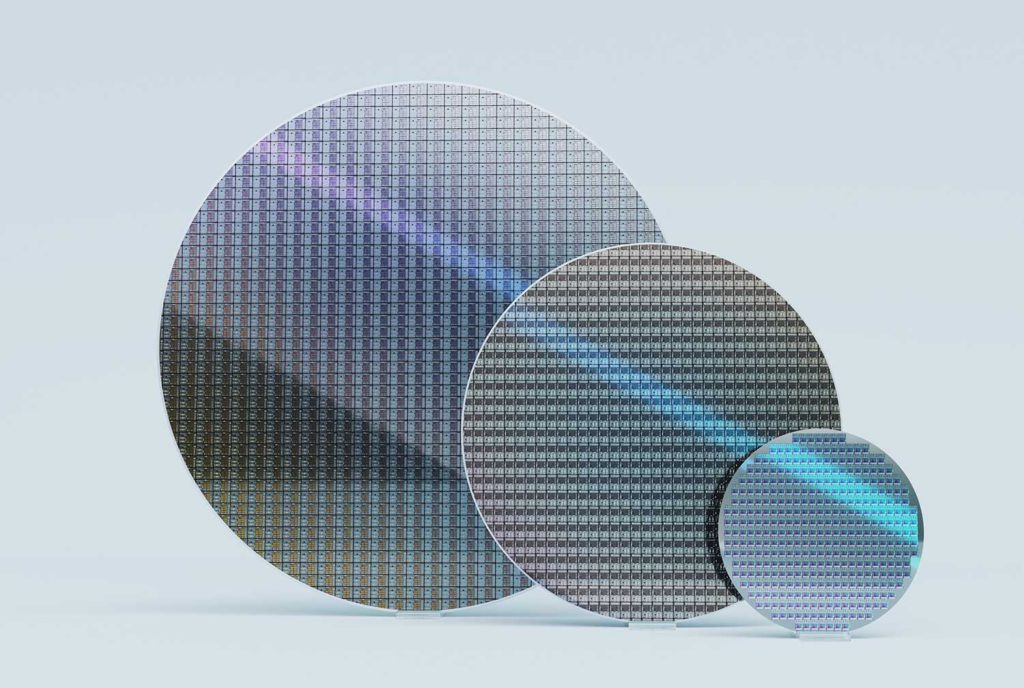
Fig. 1: 300mm wafer compared with sub-300mm wafers
While 300mm wafer fabs focus on high-performance computing and advanced logic chips, 200mm and 150mm fabs are widely used for power electronics, mixed-signal ASICs, automotive semiconductors, and IoT devices. These sub-300mm wafers offer a cost-effective and efficient manufacturing solution for industries that do not require leading-edge technology but instead prioritize analog performance, durability, and reliability
In this article, we will explore the differences between 300mm and sub-300mm wafer production, the ongoing importance of sub-300mm wafer fabs, and how RFID technology is improving sub-300mm wafer tracking and efficiency. Finally, we will highlight how SIC73F1 RFID transponders are enhancing wafer handling in sub-300mm fabs to meet the growing demand for semiconductor applications and the role of semiconductor automation in improving efficiency.
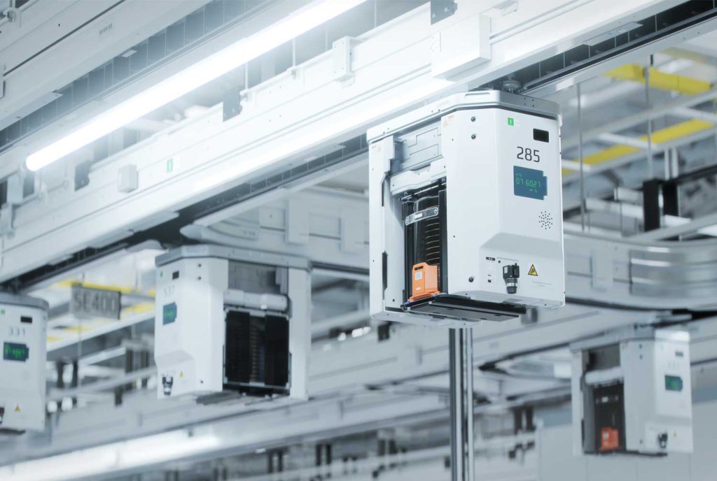
Fig. 2: 300mm wafer containers on automation line.
Understanding the Difference Between
300mm and Sub-300mm Wafer Production
The primary difference between 300mm and sub-300mm wafer production lies in automation, efficiency, and application focus.
300mm wafer fabs
- Fully automated from the outset, incorporating advanced robotics, AI-driven process optimizations, and high-throughput manufacturing systems.
- Primarily used for high-performance computing, data centers, and advanced logic semiconductor production.
- Requires sophisticated cleanroom environments and advanced wafer-handling automation systems to maintain high production efficiency.
Sub-300mm wafer fabs
- Starting before the 2000s, they are not originally designed to be fully automated.
- Include 200mm and 150mm fabs, which remain crucial for specialized semiconductor applications.
- Typically focus on power devices, mixed-signal ASICs, automotive semiconductors, IoT devices, and sensors.
- Offer a balance between cost-effectiveness and advanced capabilities, making them suitable for applications that do not require the latest manufacturing technology
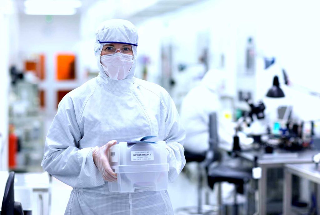
Fig. 3: An engineer carrying a sub-300mm wafer container.
Despite the advantages of 300mm fabs, non-300mm fabs remain competitive due to their ability to manufacture specialized chips at lower costs, making them indispensable to various industries. To stay relevant, these fabs are gradually integrating semiconductor automation to enhance operational efficiency.
The Trend of Sub-300mm Wafer Fabs
Sub-300mm fabs continue to play a significant role in semiconductor manufacturing. According to SEMI’s forecast, 200mm wafer production capacity is expected to expand steadily from 2025 to 2027, driven by increasing demand for power electronics, automotive applications, and IoT devices [1].
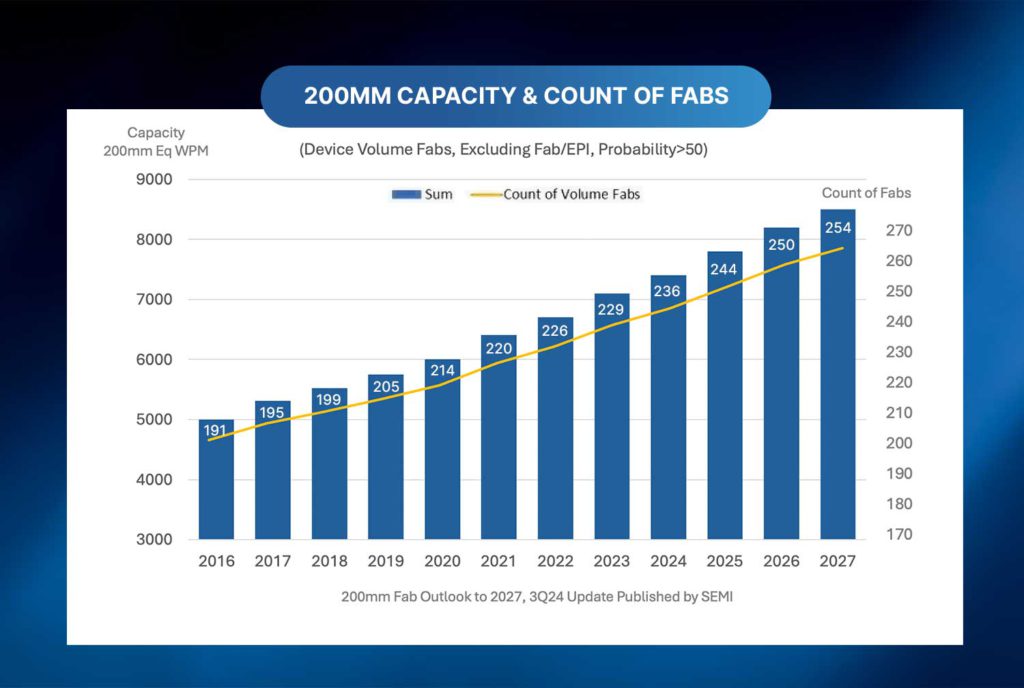
Fig. 4: SEMI’s forecast graph of 200mm semiconductor capacity & count of fabs
These fabs provide a balance between cost efficiency and technological capability, making them a preferred choice for applications such as:
- Automotive electronics: Power management ICs, microcontrollers, and safety-critical chips.
- IoT devices: Low-power sensors, RF chips, and wireless communication modules.
- Power devices: Gallium Nitride (GaN) and Silicon Carbide (SiC) semiconductors for energy-efficient power conversion.
To maintain competitiveness and scalability, these fabs are integrating modern process improvements, including semiconductor automation and data-driven optimizations to enhance manufacturing throughput and minimize errors.
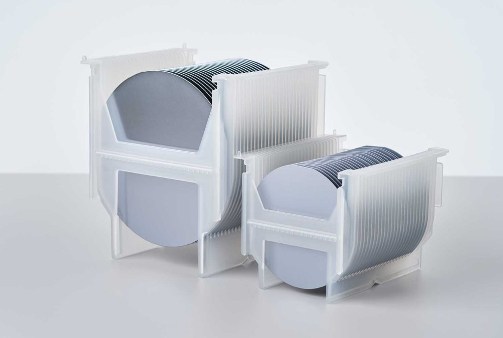
Fig. 5: Sub-300mm wafers in containers
Sub-300mm Wafer Tracking with RFID Technology
One of the key improvements in sub-300mm wafer fabs is the adoption of RFID technology for wafer tracking and handling. Unlike 300mm fabs, where automated material handling systems are standard, many sub-300mm fabs still rely on manual processes, making efficient wafer tracking critical for improving productivity and reducing human errors.
RFID technology, particularly low-frequency (LF) RFID, provides a robust solution for wafer cassette identification. Key benefits of RFID implementation in sub-300mm fabs include:
- Reliable tracking: Ensuring accurate wafer cassette identification throughout the production process.
- Improved efficiency: Reducing handling errors and streamlining material movement.
- Seamless integration: Enabling gradual adoption of automation in sub-300mm fabs.
By implementing RFID tracking in conjunction with semiconductor automation, sub-300mm fabs can enhance operational efficiency, improve yield rates, and better manage their supply chains.
Fig.6: Wafer tracking container
Enhancing Sub-300mm Wafer Handling with SIC73F1
Having already demonstrated success in 300mm wafer fabs, the SIC73F1 multi-page LF RFID transponder offers a high-efficiency solution for sub-300mm fabs. SIC73F1 can now help upgrade older generation fabs by introducing more efficient wafer tracking capabilities.
Key Features of SIC73F1
- Drop-in replacement: Conform to SEMI E144-0312 standard, ensuring compatibility with existing wafer tracking systems.
- High-memory capacity: Comes with 1,360 bits EEPROM, 17 pages read/write memory,100,000 erase/write cycles and 10 years non-volatile data retention
- Robust performance: Designed to withstand harsh semiconductor manufacturing conditions, including high temperatures, chemical exposure, and mechanical stress.
As sub-300mm fabs move toward increased automation, SIC73F1 helps bridge the gap by providing a reliable and standardized wafer tracking solution that aligns with aligns with semiconductor automation initiatives.
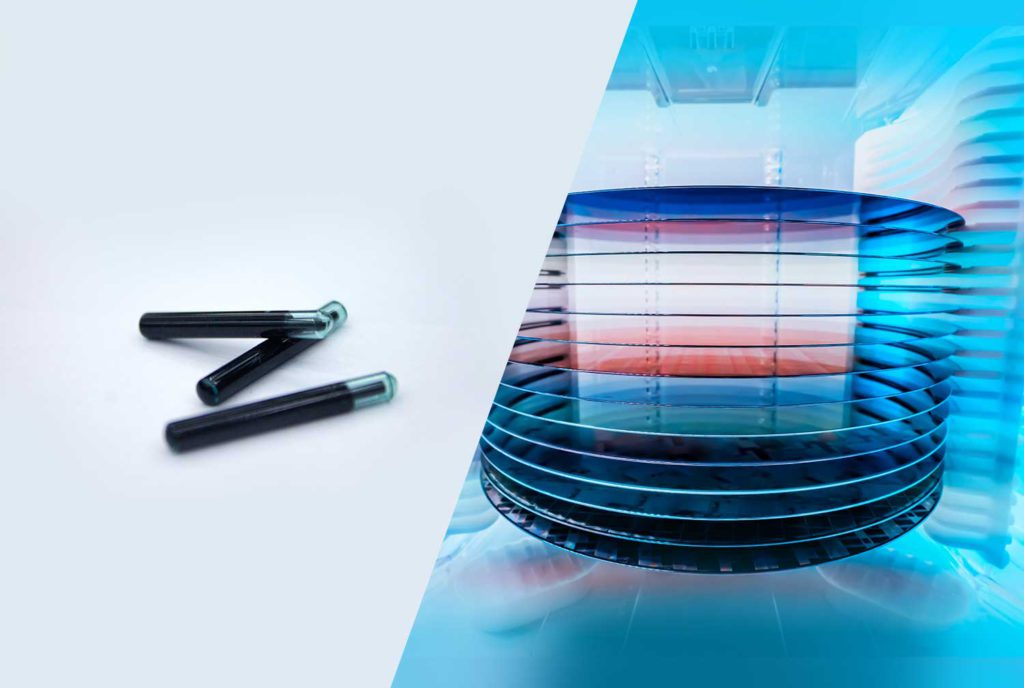
Fig.7: Wafer tracking container with Glass Tag
Conclusion
While 300mm wafer fabs dominate advanced semiconductor production, sub-300mm fabs remain essentialfor industries requiring cost-effective and specialized semiconductor solutions. As demand for power devices, automotive chips, and IoT sensors continue to grow, modernizing sub-300mm fabs through RFID tracking with SIC73F1 integration and semiconductor automation is crucial. By enhancing wafer handling efficiency and implementing gradual automation, these fabs can remain competitive and meet the evolving demands of the semiconductor industry.
References
[1] SEMI. (2024 September 25). 200mm Fab Outlook to 2027.https://www.semi.org/en/products-services/market-data/200mm-fab-outlook